
Scanning Electron Microscopy (SEM) with Focused Ion Beam (FIB)
Direct writing of nano-sized structures in 3-dimensions.
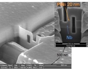
A beam of gallium ions can be used to mill a wide variety of materials with high precision inside a scanning electron microscope. The range of applications is only limited by imagination, from 3D superconducting circuits in exotic metals to "hair probes" for AFM studies. It can also be used to make cross-sectional "lamellae" for transmission electron microscopy (TEM).
Apart from the FIB source, the FEI Nova 200 system is also fitted with a platinum source, that allows deposition of Pt at desired locations (potentially interesting for e.g. making electrical contact in nanostructures). It is also equipped with a Kleindiek nanomanipulator, which has found use in the preparation of TEM lamellae and the manipulation of nanowires.
High precision fabrication requires high performance imaging. The Nova 200 system is available for standard imaging, and is capable of resolving features down to a few nanometers in size.