Electron Beam Lithography
Electrons can write patterns down to dimensions of 10 nm

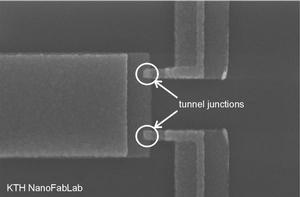
Electron beam lithography (EBL) makes use of the electron gun of a standard SEM as a direct writing tool, together with a high precision stage or "pattern generator". The diffraction limit of the wavelength of light can be avoided by writing with electrons, allowing the dimensions of the write line to be decreased to the size of the electron beam - in principle, a few nm! A graphics file is used to program the write path of the e-beam, which exposes an electron sensitive polymer.
For further information on the Raith Turnkey 150 EBL system, including a number of application reports, please refer to our technical site.