Micro- and nanofabrication enables a wide range of studies of materials confined to small dimensions where they can behave quite differently from the bulk.
The production of functional structures at the micro- and nanoscale requires three basic steps:
Thin film deposition
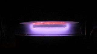
plasma glow discharge as observed in a sputter (image courtesy of University of Missouri - Kansas City)
Films of metals, metal oxides, semi-conductors and ceramics can be prepared by ion-sputtering or evaporation.
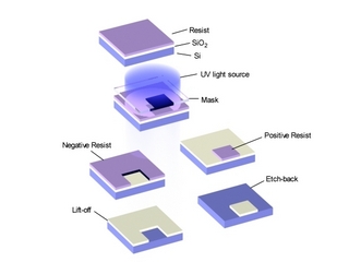
Polymeric resist films for lithography are applied via spin-coating a solution of polymer in a suitable solvent.
Patterning of the resist layer is done by exposure to radiation, either UV/visible or electrons, and then "development" of the pattern. The unreacted (or reacted) part is rinsed away with a solvent. The resulting pattern can be used to prevent deposition or etching under the masked areas. This step can be repeated multiple times.
Controlled removal of material is referred to as etching. It can be done using either "dry" reactive ion etching in a plasma reactor, or "wet" etching in a liquid that dissolves the solid material.