Materials Science
The increasing role of nanotechnology and development of novel nanomaterials require understanding of structural, mechanical and electrical properties at the nanometer-scale.
Nanomaterials
Nanoparticles, fibers and sheets (such as graphene) are employed in a wide range of applicaton areas.
Nanoparticles in high voltage cables
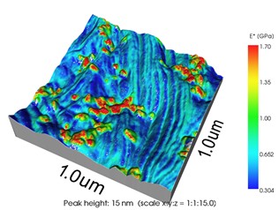
High density polyethylene is used in cables on the power grid because it can hold an extremely high AC voltage while maintaining a low current. To improve these properties even further, inorganic nanoparticles are added as "electron sinks" in the polymer matrix. Here, the distribution of hard particles is clearly visible in the much softer matrix of high density polyethylene. The nanoscale properties of the "interphase" between polymer and matrix is an area of rapidly growing interest as it is thought to have a significant effect on bulk material properties.
The image was measured with Intermodulation AFM, a powerful new technique developed at Nanostructure Physics at KTH.
Sample and measurement courtesy of Love Pallon and Ulf Gedde, Fiber and Polymer Technology, KTH
Nanocellulose membranes
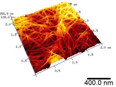
Nanocellulose is a renewable material with unique properties, of particular interest in Scandinavia, where the forest products industry is looking for new applications for their raw materials. Here, Peak Force Tapping (Bruker) accurately renders fiber dimensions and position in the membrane. Even the structure below the top layer can be well defined.
Peak Force Tapping is a method that allows soft contact at relatively low tip speeds compared with resonance-based methods. The use of soft cantilevers also allows use of very sharp tips (typically 2-5 nm) which is of benefit when characterizing nanofibers in the 10's of nanometer range.
Sample courtesy of Albert Mihranyan, Nanotechnology and Functional Materials, Uppsala University
Silicone coatings for corrosion protection
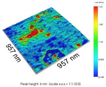
Silicones (PDMS) are a class of polymers that are finding new applications in corrosion protection. It was recently discovered that adding silica nanoparticles improves the protective properties of the coatings. Here, the mechanical nature of the composite was mapped with Intermodulation AFM. In this example, the surface viscosity is shown. It indicates that a higher viscosity is observed close to the particle-rich areas.
Sample courtesy of Hui Huang and Per Claesson at the Division of Corrosion and Surface Science, KTH
Nanotechnology
AFM and other scanning probe techniques (e.g. scanning tunneling microscopy) have been an integral part of the nanotechnology revolution, as they allow visualisation and manipulation in the boundary between continuous bulk material properties, and the "quantum region" at scales approaching molecular dimensions. The simplest application is for "super-resolution surface profiling" to quantitatively measure 3-D profiles of nano-patterned substrates. By scanning with a conducting tip, electrical properties like potential, current, capacitance and resistance can be measured. For example, scanning spreading resistance is used in the semi-conductor industry to characterize the boundary between different materials. Scanning with a magnetic tip provides a method to characterize e.g. magnetic recording media.
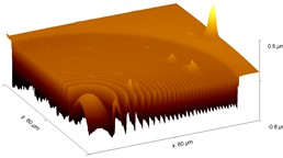
Fresnel lenses for UV optics
Fresnel lenses are used to focus UV-radiation for optical lithography. Prototype lenses are fabricated via electron beam lithography (EBL). In contrast to electron microscopy, AFM is a quantitative metrology tool that can accurately measure distances in three dimensions at high resolution, of critical imporance in many nanofabrication applications.
Sample courtesy of Wujun Mi, Medical Imaging, KTH