Our activities at KTH from 1993 on the epitaxial growth of III-V compound semiconductors for photonic devices are the continuation of those initiated at Swedish Institute of Microelectronics in the 1980’s. We carry out epitaxy of III-V semiconductor materials with a focus on semiconductor hetero- and nanostructure fabrication with subsequent device processing and characterization. We continue our strong tradition of research and innovation with a focus on devices in III-V materials for high speed lasers and photonic integrated circuits for fiber-optic communications.
The rapidly maturing crystal growth technology for III-V heterostructures has moved our research focus from conventional, nearly lattice matches structures in gallium arsenide (GaAs) and indium phosphide (InP) towards strongly lattice mismatched material combinations. One reason for this is that increased photonic integration is becoming imperative to improve functionality and decrease cost of photonic subsystems. As a consequence, we have delved into exploring III-V/Si heterojunctions both for photonics-electronics integration and photovoltaics. Besides, GaP for non-linear optics through quasi-phase matching, and III-V semiconductors as electrodes in photoelectrochemical (PEC) applications have also been added to our research portfolio. All the above-mentioned topics are enabled by our worldwide unique Hydride Vapor Phase Epitaxy (HVPE) facilitiy which combines large growth rate and high selectivity in selective area growth on planar and non-planar substrates. We collaborate with well renowned national and international research groups in device fabrication and characterization.
Axel Strömberg, Ph.D. student,
axestr@kth.se
, +46 87904417
Equipment
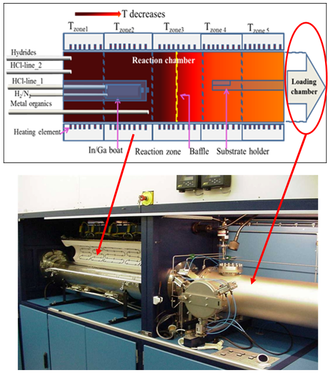
Low pressure hydride vapor phase epitaxy (LP-HVPE) reactor equipped with n-type, p- type and semi-insulating dopant sources for III-V semiconductors growth. HVPE has inherent high growth rate of III-V semiconductors up to 100 mm/hour and extremely high growth selectivity
Highlights
I. Epitaxial lateral overgrowth (ELOG) as an enabler for silicon photonics
a) Integration concept
Schematics of the Monolithic Evanescently Coupled Silicon Laser (MECSL) structure
Typical optical mode profile of the MECSL structure emitting at 1.55 micrometer from the proposed monolithically integrated structure design.
Ref: Zhechao Wang, Carl Junesand, Wondwosen Metaferia, Chen Hu, Lech Wosinski, Sebastian Lourdudoss, “III–Vs on Si for photonic applications—A monolithic approach,” Materials Science and Engineering B, vol. 177, no. 17, pp. 1551-1557 (2012)
dx.doi.org/10.1016/j.mseb.2011.12.006
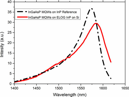
b) MWQ on ELOG InP/Si
Cross-section TEM of highly uniform InGaAsP MQWs grown on ELOG InP
Photoluminescence spectra of highly uniform InGaAsP MQWs grown on ELOG InP compared with planer InGaAsP reference
Ref: Himanshu Kataria, Wondwosen Metaferia, Carl Junesand, Chong Zhang, Nick Julian, John E. Bowers and Sebastian Lourdudoss, Simple Epitaxial Lateral Overgrowth Process as a Strategy for Photonic Integration on Silicon, IEEE JSTQE, 20(4), 8201407, 2014;
doi.org/10.1109/JSTQE.2013.2294453
c) Surface emitting 1.5 µm multi-quantum well LED on ELOG
Schematic Cross-section of MQW LED on ELOG InP/Si
RT electroluminescence of the MQW LED structure on ELOG InP/Si
Ref: Giriprasanth Omanakuttan, Yan-Ting Sun, Carl Reuterskiöld Hedlund, Carl Junesand, Richard Schatz, Sebastian Lourdudoss, Valerie Pillard, François Lelarge, Jach Browne, John Justice and Brian Corbett, Surface emitting 1.5 µm multi-quantum well LED on epitaxial lateral overgrowth InP/Si, Optical Materials Express Vol. 10(7), pp. 1714-1723 (2020);
doi.org/10.1364/OME.395249
Related publications
S. Lourdudoss, Invited, Heteroepitaxy and selective area heteroepitaxy for silicon photonics, Current Opinion in Solid State and Materials Science, vol. 16 (2), pp. 91-99, 2012;
dx.doi.org/10.1016/j.cossms.2012.01.003
Wondwosen Metaferia, Juha Tommila , Carl Junesand, Himanshu Kataria, Chen Hu, Mircea Guina, Tapio Niemi and Sebastian Lourdudoss, Selective Area Heteroepitaxy through Nanoimprint Lithography for Large Area InP on Si, Phys. Status Solidi C, vol. 9(7), pp. 1610-1613, 2012;
doi.org/10.1002/pssc.201100678
Carl Junesand, Chen Hu, Zhechao Wang, Wondwosen Metaferia, Pritesh Dagur, Galia Pozina, Lars Hultman and Sebastian Lourdudoss, Effect of the surface morphology of seed and mask layers on InP grown on Si by epitaxial lateral overgrowth, Journal of Electronic Materials, Vol. 41, No. 9, pp. 2345- 2349, 2012;
doi.org/10.1007/s11664-012-2164-9
Wondwosen Metaferia, Pritesh Dagur, Carl Junesand, Chen Hu, and Sebastian Lourdudoss, Polycrystalline indium phosphide on silicon using a simple chemical route, Journal of Applied Physics, vol. 113, p. 093504 (2013);
dx.doi.org/10.1063/1.4794006
Wondwosen Metaferia, Yan-Ting Sun, Silvia M. Pietralunga, Maurizio Zani, Alberto Tagliaferri and Sebastian Lourdudoss, Polycrystalline Indium Phosphide on Silicon by Indium Assisted Growth in Hydride Vapor Phase Epitaxy, J. Appl. Phys., 116, 033519 (2014);
dx.doi.org/10.1063/1.4890718
H Kataria, C Junesand, Z Wang, W Metaferia, Y T Sun, S Lourdudoss, G Patriarche, A Bazin, F Raineri, P Mages, N Julian,and J E Bowers, Towards a monolithically integrated III–V laser on silicon: optimization of multi-quantum well growth on InP on Si, Semicond. Sci. Technol. 28, 094008, 2013;
doi.org/10.1088/0268-1242/28/9/094008
Carl Junesand, Himanshu Kataria, Wondwosen Metaferia, Nick Julian, Zhechao Wang, Yan-Ting Sun, John Bowers, Galia Pozina, Lars Hultman, and Sebastian Lourdudoss, Study of planar defect filtering in InP grown on Si by epitaxial lateral overgrowth, Optical Materials Express, Vol. 3, Issue 11, pp. 1960- 1973 (2013);
dx.doi.org/10.1364/OME.3.001960
Carl Junesand, Ming-Horn Gau, Yan-Ting Sun, Sebastian Loududoss, Juan Jimenez, Pablo Aitor Postigo, Fransisco Miguel Morales Sánchez, Jesus Hernandez, Sergio Molina, Aouni Abdessamad and Pirouz Pirouz, Defect reduction in heteroepitaxial InP on Si by epitaxial lateral overgrowth, Mater.Express,Vol.4(1), 41-53, 2014;
doi.org/10.1166/mex.2014.1140
Wondwosen Metaferia, Apurba Dev, Himanshu Kataria, Carl Junesand, Yan-Ting Sun, Srinivasan Anand, Juha Tommila, Galia Pozina, Lars Hultman, Mircea Guinb, Tapio Niemi and Sebastian Lourdudoss, High Quality InP Nanopyramidal Frusta on Si, CrystEngComm, 2014;
doi.org/10.1039/C3CE42231C
Yan-Ting Sun, Carl Junesand, Wondwosen Metaferia, Himanshu Kataria, Nick Julian, John Bowers, Galia Pozina, Lars Hultman, and Sebastian Lourdudoss, Optical and Structural properties of Sulfur-doped ELOG InP on Si, J. Appl. Phys. 117, 215303 (2015);
dx.doi.org/10.1063/1.4921868
Juliana Jaramillo-Fernandez, Emigdio Chavez-Angel, Reza Sanatinia, Himanshu Kataria, Srinivasan Anand, Sebastian Lourdudoss and Clivia M. Sotomayor-Torres, Thermal conductivity of epitaxially grown InP: experiment and simulation, CrystEngComm., vol 19, pp. 1879-1887, 2017;
doi.org/10.1039/C6CE02642G
II. III-V/Si heterojunction and photodiode
a) InP/Si heterojunction photodiode fabricated by corrugated epitaxial lateral overgrowth (CELOG)
SEM cross-section of CELOG n-InP/p-Si heterojunction
I-V curve of the photodiode under dark and illumination conditions
Ref.: Y.T. Sun, G. Omanakuttan, and S. Lourdudoss, An InP/Si heterojunction photodiode fabricated by self- aligned corrugated epitaxial lateral overgrowth; Appl. Phys. Lett. 106, 213504 (2015);
dx.doi.org/10.1063/1.4921992
b) Epitaxially fused GaInP/Si heterojunction
(a) HRTEM image of the CELOG GaInP/Si heterojunction. (b)–(e) EDS images of Si, Ga, In, and P. (f ) EDS spectrum of the CELOG GaInP/Si interface. (g) FFT image of (a).
Ref.: Chengru Wang, Giriprasanth Omanakuttan, Leilei Xu, Tong Liu, Zengli Huang, Sebastian Lourdudoss, Chaoying Xie, Yan-Ting Sun, Optical and interfacial properties of epitaxially fused GaInP/Si heterojunction, Journal of Applied Physics 128, 055308 (2020);
doi.org/10.1063/1.5141510
Related publications
Wondwosen Metaferia, Himanshu Kataria, Yan-Ting Sun and Sebastian Lourdudoss, Growth of InP Directly on Si by Corrugated Epitaxial Lateral Overgrowth, IOP Journal of Physics D: Appl. Phys. 48 (2015) 045102;
doi.org/10.1088/0022-3727/48/4/045102
Giriprasanth Omanakuttan, Stamoulis Stergiakis, Abhishek Sahgal, Ilya Sychugov, Sebastian Lourdudoss, and Yan-Ting Sun, Realization of GaxIn1-xP/Si hetero-interface by corrugated epitaxial lateral overgrowth, Phys. Status Solidi A, 1600631 (2017);
doi.org/10.1002/pssa.201600631
Giriprasanth Omanakuttan, Oscar Martínez Sacristán, Saulius Marcinkevičius, Tomas Kristijonas Uždavinys, Juan Jiménez, Hasan Ali, Klaus Leifer, Sebastian Lourdudoss, and Yan-Ting Sun, Optical and interface properties of direct InP/Si heterojunction formed by corrugated epitaxial lateral overgrowth, Optical Materials Express, 9(3), 1488-1500 (2019);
doi.org/10.1364/OME.9.001488
Axel Strömberg, Giriprasanth Omanakuttan, Yingjun Liu, Tangjie Mu, Zhehan Xu, Sebastian Lourdudoss, Yan-Ting Sun, Heteroepitaxy of GaAsP and GaP on GaAs and Si by low pressure hydride vapor phase epitaxy, J. Crystal Growth, Vol 540, p. 125623 (2020);
doi.org/10.1002/pssa.201900627
Axel Strömberg, Prakhar Bhargava, Zhehan Xu, Sebastian Lourdudoss and Yanting Sun, Direct Heteroepitaxy and Selective Area Growth of GaP and GaAs on Si by Hydride Vapor Phase Epitaxy, Physica Status Solidi (a), 2020, 2000447;
doi.org/10.1002/pssa.202000447
III. Buried heterostructure quantum cascade lasers
a) Buried ridge structure
Buried heterostructure quantum cascade laser (BH-QCL) emitting at 4.7 µm
Output power and wall-plug efficiency for various ridge widths of BH-QCL under CW operation
Ref: W. Metaferia, B. Simozrag, C. Junesand, Y.T. Sun, M. Carras, R. Blanchard, F. Capasso and S. Lourdudoss, Demonstration of a quick process to achieve buried heterostructure quantum cascade laser leading to high power and wall plug efficiency, Optical Engineering, 53(8), 087104, 2014;
doi.org/10.1117/1.OE.53.8.087104
b) Buried heterostructure photonic crystal QCLs with 5W surface emission
I-V-L curve of the buried heterostructure photonic crystal QCL with ~8.75 µm light emission collected from the surface
SEM cross-section of the PhC layer consisting of a square lattice of active-region (InGaAs/AlInAs) pillars (red) surrounded by HVPE regrown semi- insulating InP:Fe
Ref: Zhixin Wang, Yong Liang, Bo Meng, Yan-Ting Sun, Giriprasanth Omanakuttan, Emilio Gini, Mattias Beck, Ilia Sergachev, Sebastian Lourdudoss, Jérôme Faist and Giacomo Scalari, Large area photonic crystal quantum cascade laser with 5 W surface-emitting power, Optics Express, Vol. 27, No. 16, pp. 22708-22716 (2019);
doi.org/10.1364/OE.27.022708
Related publications
Qiye Zheng, Honggyu Kim, Runyu Zhang, Mauro Sardela, Jianmin Zuo, Manavaimaran Balaji, Sebastian Lourdudoss, Yan-Ting Sun, and Paul V. Braun, Epitaxial growth of three dimensionally structured III-V photonic crystal via hydride vapor phase epitaxy, Journal of Applied Physics, vol. 118(22), 224303 (2015);
doi.org/10.1063/1.4937273
R. Peretti, V. Liverini, M.J. Süess, Y. Liang, P-B. Vigneron, J. M. Wolf, C. Bonzon, A. Bismuto, W. Metaferia, M. Balaji, S.Lourdudoss, E. Gini, M. Beck and J. Faist, Room Temperature Operation of a Buried Heterostructure Photonic Crystal Quantum Cascade Laser, Laser & Photonics Reviews, 10(5), 843-848 (2016);
doi.org/10.1002/lpor.201600047
Martin J. Süess, Romain Peretti, Yong Liang, Johanna M. Wolf, Christopher Bonzon, Borislav Hinkov, Selamnesh Nida, Pierre Jouy, Wondwosen Metafeira, Sebastian Lourdudoss, Mattias Beck, Jérôme Faist, Advanced fabrication of single-mode and multi-wavelength MIR-QCLs, Photonics 2016, 3, 26;
doi.org/10.3390/photonics3020026
Xiaodan Pang, Oskars Ozolins, Richard Schatz, Joakim Storck, Aleksejs Udalcovs, Jaime Rodrigo Navarro, Aditya Kakkar, Gregory Maisons, Mathieu Carras, Gunnar Jacobsen, Sergei Popov and Sebastian Lourdudoss, Gigabit free-space multi-level signal transmission with a mid-infrared quantum cascade laser operating at room temperature, Optics Letters, Vol. 42 (18), 3646-3649 (2017);
doi.org/10.1364/OL.42.003646
Feature Article: Xiaodan Pang, Oskars Ozolins, Lu Zhang, Richard Schatz, Aleksejs Udalcovs, Xianbin Yu, Gunnar Jacobsen, Sergei Popov, Jiajia Chen, Sebastian Lourdudoss, Free‐Space Communications Enabled by Quantum Cascade Lasers, Phys. Status Solidi A 2020, 2000407;
doi.org/10.1002/pssa.202000407
Jae Ha Ryu, Jeremy D. Kirch, Benjamin Knipfer, Zerui Liu, Morgan Turville-Heitz, Tom Earles, Robert A. Marsland, Axel Strömberg, Giriprasanth Omanakuttan, Yan-Ting Sun, Sebastian Lourdudoss, Dan Botez, and Luke J. Mawst, Beam stability of buried-heterostructure quantum cascade lasers employing HVPE regrowth, Optics Express, 29(2) 2819-2826 (2021);
doi.org/10.1364/OE.414489
IV. Quasi-phase matched orientation-patterned GaP heteroepitaxially grown on OP-GaAs
HVPE grown on OP-GaP on OP-GaAs template; A and B are demarcations of domain boundaries
Real part of conductivity vs THz frequency of bulk GaP grown by HVPE; Red curve fitted to Drude model
Ref: Axel Strömberg, Giriprasanth Omanakuttan, Tangjie Mu, Pooja Vardhini Natesan, Tajka Syeed Tofa, Myriam Bailly, Arnaud Grisard, Bruno Gérard, Hoon Jang, Valdas Pasiskevicius, Fredrik Laurell, Sebastian Lourdudoss, and Yan-Ting Sun, Direct Heteroepitaxy of Orientation-Patterned GaP on GaAs by Hydride Vapor Phase Epitaxy for Quasi-Phase-Matching Applications,
Phys. Status Solidi A, 2019, 1900627;
doi.org/10.1002/pssa.201900627
Current projects
2021-2023: STINT-NSFC, Photoelectrocatalytic CO2 reduction on III-V/Si/TMP composite photoelectrode
2021-2022: Olle Engqvist Foundation, Orientation-patterned GaP on Si for entangled photon source in integrated quantum photonics
2020-21: Swedish Research Council (VR), Indo-Swedish joint network grant, Bulk crystal growth of Ga2O3 and fabrication of heterojunction diodes
2019-2022: EU Horizon 2020 FETOPEN, No. 828893, cFLOW -Coherent ultraFast Long Wave infrared communications
2017-2021: High-efficiency multijunction solar cells on silicon, Swedish Energy Agency
2016-2021: Knut and Alice Wallenberg Foundation, Photonic Quantum Information
Collaborations
Quasi-phase matched III-V semiconductors
Fredrik Laurell and Valdas Pasiskevicius, Laser Physics, KTH
Mohamed Bourennane, Stockholm University
Arnaud Grisard and Bruno Gérard, Thales Research & Technology, Palaiseau, France
Solar cell
Mattias Hammar, EECS School, KTH
QCL
Richard Schatz, Xiaodan Pang and Sergei Popov, Applied Physics, KTH
Jérôme Faist, ETH, Zurich, Switzerland
Luke Mawst, Wisconsin University
Aléxandre Delga, III-V labs, Paris, France
Mathieu Carras, Mirsense, Paris, France
Photoelectrocatalytic CO2 reduction :
Peng Zhang, Shanghai Jiao Tong University, Shanghai, China